
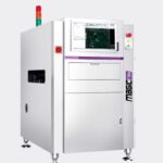
V5300 Double-Side Wave soldering Inspection Inline AOI
Advanced Hardware Structure
■ Industrial Camera + Telecentric Lens
The high component solder joint inspection is not affected as no shadow effect in the entire filed of view.
■ The Double-side Camera Synchronizes The X-Y
Movement, Asynchronous Acquire The Image Perform the inspection on both sides simultaneously, and
the light source does not interfere with each other, the inspection speed reaches the highest.
Core Technology and Advantages
■ Intelligent Solder pad positioning + Entire FOV Assist Positioning
- Solder pad position able to reduce high false call due to deformation of PCB after reflow, especially for FPC.
- For non FPC, entire FOV assist positioning is the perfect solution to reduce the high false call due to PCB warp, silkscreen, interference of the board’s legend.
- High detection ability on no exposed pad components (BGA,etc.) or partially shielded components.
■ Poor Soldering Inspection
Based on precisely positioning on the solder pad, the features points of the entire solder pad will be analyzed. Therefore, the poor solder of chip or IC can be effectively detected.
■ Detection Parameters Directly Interface with IPC
Standards
Based on the IPC test standard, the test results are more
reliable.Shift: IPC-A-610-G Class 3 – If the component shift out of solder pad more than 25% of the component electrode, it will be NG.
■ Special Wave Soldering Algorithm for DIP Inspection Special wave soldering algorithm on hand insert and machine insert DIP inspection.
■ Other Advantages
Intelligent programming (One click rectification, Add substitute, Sub-programming ,etc.); Offline programming and fine tuning in real time without stopping the production line; Remote technical support.